【学生体験談】JoinTECH-Visitでバレンシア大学に留学
Student Reports: Two KIT Master’s Students Sent to the University of Valencia through JoinTECH-Visit
| 派遣学生 / Participants | 博士前期課程 電子システム工学専攻 2名 / Two master’s students in Electronics. |
|---|---|
| 期間 / Period | 令和7年6月19日~7月8日 / June 19, 2025 – July 8, 2025 |
| 派遣先 / Host University |
バレンシア大学(スペイン) / University of Valencia(Spain) |
【学生体験談1】
2025/6/19~2025/7/8までJoinTECH-Visitにて、バレンシア大学へ研究留学に参加しました。現地の研究室の見学およびデモンストレーションを行い、MO-CVDによる薄膜成長やバルク単結晶成長について学びました。
今回の経験は、これまで自分が扱ってきた装置や手法とは異なる設備や方法論に直接触れる機会を得たことで、教科書や論文から得られる知識を超えた、非常に貴重な実践的知識をもたらしました。
さらに、国際会議への参加により、最先端の半導体研究に幅広く触れることができました。特に、薄膜成長や界面特性評価など、自身の専門分野以外の領域について理解を深められた点は、大きな刺激となりました。英語での質疑応答に参加したことも、語学面で大きな挑戦であり、同時に非常に意欲を高める経験となりました。この経験は、今後の英語学習への大きな原動力になると確信しています。
上述のとおり、多様な学びの機会を得られたことに加えて、バレンシアは安全な都市であり、食事も非常に美味しく、口に合うものでした。バレンシアでは、学校を除き、スーパーなど日常生活に関わる多くの人々はスペイン語のみを話します。ちょっとしたコツとして、
「Gracias(ありがとう)」
「Pague con tarjeta(カードで支払います)」
「Quiero una bolsa, por favor(袋をください)」といった表現を覚えておくと便利です。
(博士前期課程 電子システム工学専攻 1年次 Hさん)
Student Report 1:
I participated in a research stay at the University of Valencia under the JoinTECH-Visit program in June. I participated in a research stay at the University of Valencia in June under the JoinTECH-Visit program. During the stay, I observed and received demonstrations of laboratory research activities, including thin-film growth using MO-CVD and bulk single-crystal growth techniques.
This experience provided invaluable practical knowledge that went beyond what could be learned from textbooks or papers, as it involved direct exposure to equipment and methodologies distinct from those I was familiar with.
Furthermore, attending international conferences offered broad exposure to cutting-edge semiconductor research. It was incredibly stimulating to deepen my knowledge in areas outside my specific specialization, particularly in thin-film growth and the evaluation of interface properties. I participated in a research stay at the University of Valencia in June under the JoinTECH-Visit program. During the stay, I observed and received demonstrations of laboratory research activities, including thin-film growth using MO-CVD and bulk single-crystal growth techniques.
As mentioned above, I have received a variety of learning opportunities. In addition to that, Valencia is a safe city, and as for the food, it was delicious and well suited to my taste.
In Valencia, with the exception of schools, most people involved in daily life, such as those in supermarkets, speak only Spanish. As a little tip, it is useful to remember “Gracias (Thank you)”,” Pague con tarjeta (Pay by credit card)”,” Quiero una bolsa, por favor (Please give me a bag).
(H, 1st year Master’s Student in Electronics)
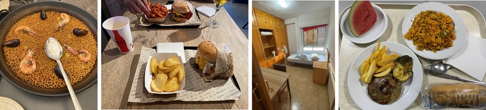
左から:バレンシアのビーチ沿いのレストラン(パエリアはほぼ毎日食べました)
Restaurants by the beach in Valencia(I ate paella almost every day)
大学の食堂/University cafeteria 、大学の寮/Student dormitory
過去にスペインへ留学していた先輩に勧められた「Hundred Burgers」というレストラン
“Hundred Burgers,” a restaurant recommended by a senior who had previously studied in Spain.
【学生体験談2】
私は6月にスペインのバレンシア大学において、3週間のJoinTECH-Visitに参加しました。ここでは、そこで得た経験と学びをまとめ、今後参加を検討する学生に本プログラムの価値を共有したいと思います。
私はミストCVD(mist-CVD)法を用いた薄膜作製を専門としています。本訪問の主な目的は、薄膜作製技術および評価手法に関する知識を深めることでした。日本での研究では、比較的簡便で特定の酸化物薄膜に適したミストCVD法を用いていますが、バレンシア大学では、より高度な手法である金属有機化学気相成長法(MOCVD)が用いられています。この手法は成膜条件をより精密に制御でき、特に化合物半導体分野において半導体産業で広く活用されています。
滞在中、MOCVD装置の稼働を間近で見学するという貴重な機会を得ました。さらに、研究室ミーティングにも参加し、高分解能X線回折(XRD)装置やホール効果測定装置など、薄膜評価に用いられる各種装置も見学しました。これらの交流は技術的理解を広げるとともに、自身の研究に対する新たな着想を与えてくれました。
本プログラムの大きなハイライトの一つは、スペインで開催された国際学会への参加でしたヨーロッパ各地から集まった研究者が、半導体、材料科学、電子デバイスに関する研究成果を発表していました。
私自身は発表者ではありませんでしたが、積極的に質問や議論に参加しました。多様な背景を持つ研究者と英語で議論する経験は、自信の向上および科学的内容を簡潔かつ明確に伝える能力の向上につながりました。また、材料安定性や界面制御といった共通課題に対する各国の研究アプローチを知ることで、自身の研究に新たな視点を得ることができました。
日常生活ではスペイン語が主に使用されるため、言語面での困難もありましたが、多くの学生や研究者が英語を話し、非常に親切に対応してくださいました。こうした交流を通じて、多様な文化や価値観への理解を深め、新しい環境へ適応する力を養うことができました。
本短期交換プログラムは、学術的にも個人的にも大きな影響を与える経験となりました。海外で研究活動を行うことで、専門知識の拡充、コミュニケーション能力の向上、そしてよりグローバルな視野の獲得につながりました。MOCVD装置のような先端設備を実際に見学した経験は、自身の研究手法を再考する契機となり、今後の実験への応用も検討しています。
留学を検討している学生には、ぜひ挑戦することを強く勧めます。言語の壁や文化の違い、研究環境の差異などの課題はありますが、それらはすべて成長の機会です。特に英語による意思疎通能力や基礎知識を事前に十分準備しておくことで、滞在期間をより有意義なものにできるでしょう。
わずか3週間という短期間でしたが、科学技術のみならず、自身や世界について多くを学ぶことができました。この経験は、今後の学術的および職業的キャリアにおいて、長く活きる貴重な財産となるものです。
(博士前期課程 電子システム工学専攻 1年次 Sさん)
Student Report 2:
I participated in a three-week JoinTECH-Visit program at the University of Valencia in Spain. This report summarizes the experiences I gained and the lessons I learned, aiming to share the value of this program with future students.
I specialize in thin-film fabrication using the mist chemical vapor deposition (mist-CVD) method. The primary focus of my visit was to deepen my knowledge of thin-film fabrication techniques and evaluation methods. While my current research in Japan utilizes the mist-CVD method, which is relatively simple and suitable for certain oxide films, the University of Valencia employs a more advanced technique: metal-organic chemical vapor deposition (MOCVD). This method allows for much finer control over deposition parameters and is widely used in the semiconductor industry, particularly for compound semiconductors.
During my stay, I had the rare opportunity to closely observe the MOCVD system in operation.
Furthermore, I participated in lab meetings and visited other equipment used for evaluating thin films, including high-resolution XRD and Hall effect measurement systems. These interactions expanded my technical understanding and provided inspiration for my own experiments.
One of the highlights of the program was attending an international conference held in Spain, where researchers from across Europe presented their work on semiconductors, materials science, and electronic devices.
Although I was not presenting myself, I actively participated by asking questions and joining discussions. The experience of communicating in English with researchers from various backgrounds helped me build confidence and improve my ability to express scientific ideas clearly and concisely. I also learned how different research environments approach common challenges, such as material stability or interface control, which gave me new perspectives on my own work.
Life in Valencia was both exciting and educational. The city itself is rich in culture and history, with beautiful architecture, delicious food, and a relaxed atmosphere. I especially enjoyed exploring the historic center, visiting the City of Arts and Sciences, and trying local dishes like paella.
Language was sometimes a challenge, as Spanish is the dominant language in daily life. However, many students and researchers spoke English, and I found that people were very helpful and welcoming. Through these interactions, I gained a deeper appreciation for different cultures and values, and I learned to adapt to new environments quickly.
This short-term exchange program has had a profound impact on me, both academically and personally. By experiencing research in a foreign country, I was able to broaden my scientific knowledge, improve my communication skills, and develop a more global perspective. Observing advanced equipment such as MOCVD systems firsthand has inspired me to consider new approaches in my own research, and I am already thinking about how to integrate these insights into future experiments.
To students considering a study abroad opportunity, I wholeheartedly encourage you to take the leap. While there may be challenges—language barriers, cultural differences, or unfamiliar systems—each of these is an opportunity to grow. Preparing well in advance, especially in terms of English communication and background knowledge, will help you make the most of your time abroad.
In just three weeks, I learned more than I expected, not only about science and engineering but also about myself and the world. It was a truly valuable experience that I will carry with me throughout my academic and professional career.
(S, 1st year Master’s Student in Electronics)
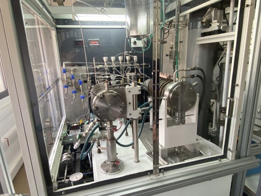
金属有機化学気相成長法システム
MOCVD system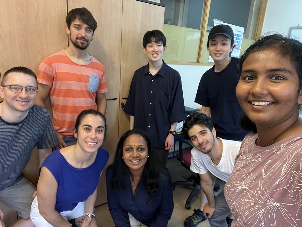
バレンシア大学の研究室メンバーと
Lab members at University of Valencia